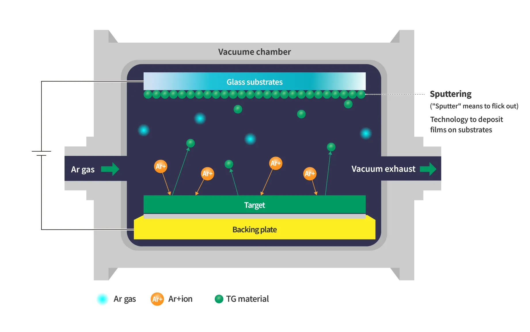
Thin Film Formation by Sputtering
Sputtering is a widely used PVD (Physical Vapor Deposition) technology for forming high-quality thin films. In this process, argon (Ar) gas is ionized in a vacuum chamber, and the resulting ions bombard a target material, causing material particles to be ejected and deposited onto a substrate to form a thin film.
Sputtering targets are typically circular or rectangular plates bonded to backing plates with high precision. Target quality directly influences film thickness uniformity, composition control, and device performance, making sputtering targets essential for a wide range of applications, including displays, semiconductors, optical components, and other advanced electronic devices.
Leveraging extensive expertise in materials such as ITO and IGZO, Mitsui Kinzoku develops and supplies high-quality sputtering targets worldwide, supporting customers' development of next-generation devices.