

Contributing to Device Downsizing
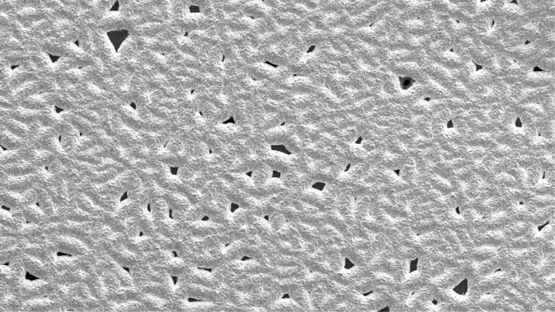
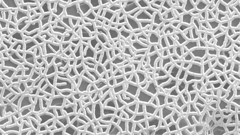
Compared with perforated foils produced by conventional processing methods such as punching or laser processing, this technology enables thin copper foil with a high open area ratio and fine hole diameters. As a result, it contributes to the downsizing and thinning of devices. Because this manufacturing method is less likely to generate burrs or other protrusions, it also reduces the risk of short circuits caused by contact or dendrite formation, even when the distance between copper foils is narrowed in applications that require a layered structure.
Technology and Features
Perforated Copper Foil Produced Only through an Electrolytic Process, without Post-Processing
All of our copper foil products are manufactured using an electrolytic copper foil process. Using a process similar to that used for our other copper foil products, perforated copper foil can be produced without post-processing, simply by controlling the deposition state. Unlike conventional perforated foil produced by post-processing, this method forms holes at the same time as the copper foil is deposited. This makes it possible to create thinner foil with smaller holes at a higher density.
Application Examples
This technology is expected to be applied to power generation and energy storage devices that require electrical current to flow or be collected while allowing fluids such as liquids and gases to pass through. In addition, because it has a high specific surface area, it can also be used as a thin, flexible porous material that does not shed powder. Please consider its potential use as a catalyst or catalyst support.

Contact